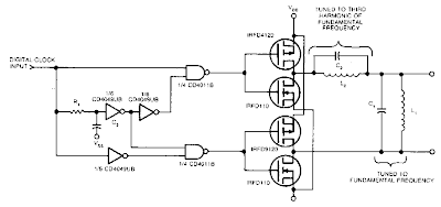
Build a Square A to Sine Wave Converter Circuit Diagram. This is a simple circuit diagram in this circuit using Two pairs of MOSFETs form a bridge that alternately switches current in opposite directions. Two parallel-resonant LC circuits complete the converter. The Ll/C1 combination is resonant at the fundamental frequency; the L2/C2 combination is resonant at the clock frequency`s third harmonic and acts as a trap.
Square A to Sine Wave Converter Circuit Diagram

Tl and C3 ensure that both halves of the MOSFET bridge are never on at the same time by providing a common delay to the gate drive of each half. Select the values of R1 and C3 to yield a time constant that`s less than 5% of the clock`s period. You can add an output amplifier for additional buffering and conditioning of the circuit`s sine-wave output.
Comments
Post a Comment